Morphology measurement
A measurement of the surface topography and the subsequent evaluation of length dimensions is by far the most wanted requirement
on a measurement with a high resolution. The nanometrology methods can be used in microelectronics, optics, biology, particle analysis and many other
disciplines.
The most often used device for this kind of measurements is the Atomic Force Microscope (AFM) capable
of data acquisition which represent a surface morphology even with atomar resolution on a area having 0.1x0.1 mm (even more in case of special devices). For the measurement of 3D structures it is possible to use a nanoCMM (a coordinate measuring
device). Of course, the morphology can be measured also by other methods such as confocal or electron microscopy. These approaches are however
generaly not so advanced considering the traceability and metrology compared to devices based on the contact principle which is the case of
the AFM. But we can observe a massive development of these methods and in the future especially the electron microscopy will play an important role
in the nanometrology.
The main criterion in choosing an AFM or a coordinate measuring machine is the shape of the measured structure. It is possible
to use the AFM only for the charatecterization of planar structures with a limited range of heights (ca 10 µm for commercial systems).
It is possible to further process the data acquired by the microscope and except for dimension
evaluation it is possible to get also another type of information: roughness, waviness, grain or particle size, distribution of heights and slopes,
fractal properties, etc.
From the metrology point of view it is necessary to understand the way the result is generated within such an analysis and to
correctly determine its uncertainty which can be a difficult task (e.g. in fractal analysis). The evaluation of data resulted from morphology
measurements on the nano- and microscale is therefore one of the research areas of the nanometrology. The open source program
Gwyddion is one of the possibilities of how to perform a data analysis. In contrast to proprietary programs it is
possible to view the source code and hence to understand the detailed functionality of the software. |
 |
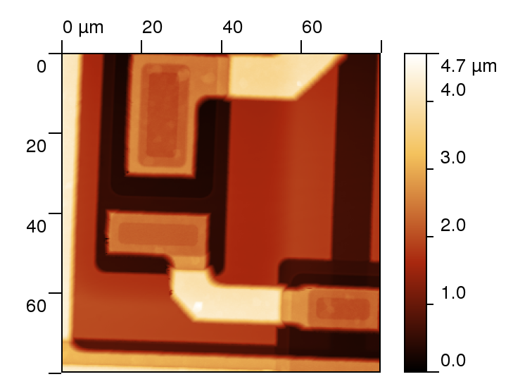
| AFM image of a surface of a microelectronic component |
In order to ensure the traceability of the surface shape measurement it is possible to use two methods:
- calibration of the microscope or coordinate measuring machine with samples with known dimensions,
- direct use of traceable sensors (e.g. interferometers) in the measuring device.
 |
The combined use of calibrated samples and commercial devices enables to reach an accuracy on the order of tenths of a percent. The accuracy of uncalibrated commercial devices is much worse, typically on the order of units of percents. In order
to reach lower uncertainty the metrology institutes prefer the second method. This however means to build a dedicated device. Special metrological
microscopes can be found in the majority of metrology institutes within European countries.
The uncertainty of length measurements in metrology institutes is typically on the order of units of nanometers depending on the shape of the measured structure.
|
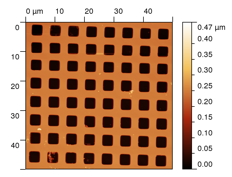
| AFM image of a calibration grating |
We focus in our department on the development of methods for statistical analysis of surface roughness and evaluation
of uncertainties related to this type of AFM data evaluation. Furtermore, we develop microscopes for morphology measurements on large areas and for
measurements with a very small uncertainty and also software tools for data evaluation and uncertainty calculation.
|

