Temperature and thermal conductivity
Thermal loses are one of the main factors limiting the miniaturization of microelectronics. During electric current flowing
through microelectronic circuits nearly all power is converted to heat which is necessary to sink. The smaller the integrated circuit is the more
constrained are the possibilities of heatsinking. Heating of the circuit means not only that the electric power is consumed but also that the error
rate of signal processing is higher. It is therefore necessary to minimalize the heat generation and/or consumption.
Until the sizes of microelectronic devices were on the order of microns it was possible to
observe the local temperature distribution e.g. by a infrared camera. The resolution of such conventional methods cannot be better than some microns
by principle. The solution is to use the scanning probe microscopy, in particular a Scanning Thermal Microscopy (SThM).
With a special probe we are able to measure simultaneously shape of the surface and its temperature with lateral resolution of several tens of
nanometers and thermal resolution on the order of tenths of a Kelvin.
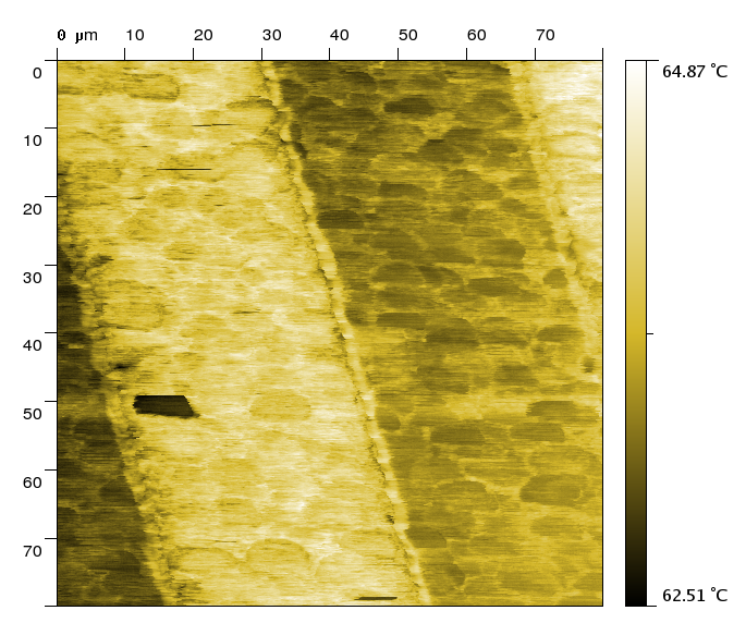
The image shows a surface of heated microstructured hydrogen sensor. The apparent temperature difference between the platinum and
ceramic part of the sensor is caused by the difference in emissivity of both surfaces - the ceramic surface emits more heat and is therefore cooler.
|
 |
| Temperature mapping of a hydrogen sensor surface |
Another physical quantity which can be acquired by the scanning thermal microscope is the thermal
conductivity. This quantity plays an important role in the microelectronic components manufacture and design of different nanocomposite materials. The
knowledge of this quantity is important when manufacturing materials having both a large thermal conductivity or perfect isolating properties. Even
here it is possible to say that none of the conventional methods provides higher lateral resolution. On the other hand, the SThM method is rather far
away from being a quantitative analysis (the calibration is dependent on the use of special samples, we observe many systematic errors during the
measurement), therefore for larger samples or samples that are not microstructured it is better to use a conventional method.
|

