Optical properties
Considering a local analysis of optical properties we have to mention the fundamental limit which is the wavelength of the light
used for the sample analysis. The highest possible optical resolution that we can achieve is limited by the diffraction to approximately one half
of the wavelength and it is impossible to break this limit by conventional approaches. In nanometrology the standard devices using light
(reflectometer or ellipsometer) are therefore limited with a resolution on the order of several hundreds of nanometers. Note that this limitation
is related to the lateral resolution and that for example a thickness of a thin film can be determined with an uncertainty of several nanometers
using these methods.
But even in this type of characterization we are able to acquire an interesting information on the microscale and partially
also on the nanoscale. Using scanning or mapping reflectometry or ellipsometry we can measure e.g. the distribution of index of refraction on
optoelectronic devices or planar light guides. These analytical methods are well known have been developed for more than hundred years and the
uncertainty of the optical measurements can be on the order of one tenth or one hundredth of a percent.
Nevertheless, if we want to go down with the resolution to some nanometers we have to change the measurement
strategy completely. One of the possibilities is to use a source or a light detector located in a close proximity to the surface. This is the case of
a Scanning Near-Field Optical Microscopy (SNOM). The probe in the SNOM is formed by a optical fiber
with aperture of 50-100 nm and is used to emit or to collect the light
Although the SNOM is definitely a revolutionary technique with respect to its resolution and that has a huge response by e.g. biologists in the 80's of the last century when it was rediscovered, the data interpretation is much more complicated compared to the conventional
methods mentioned above. The interaction between the probe and the surface is rather complex problem and it is necessary to perform various numerical
computations in order to understand it. Another issue is the probe geometry that is unknown in principle and can alter during the measurement.
|
 |
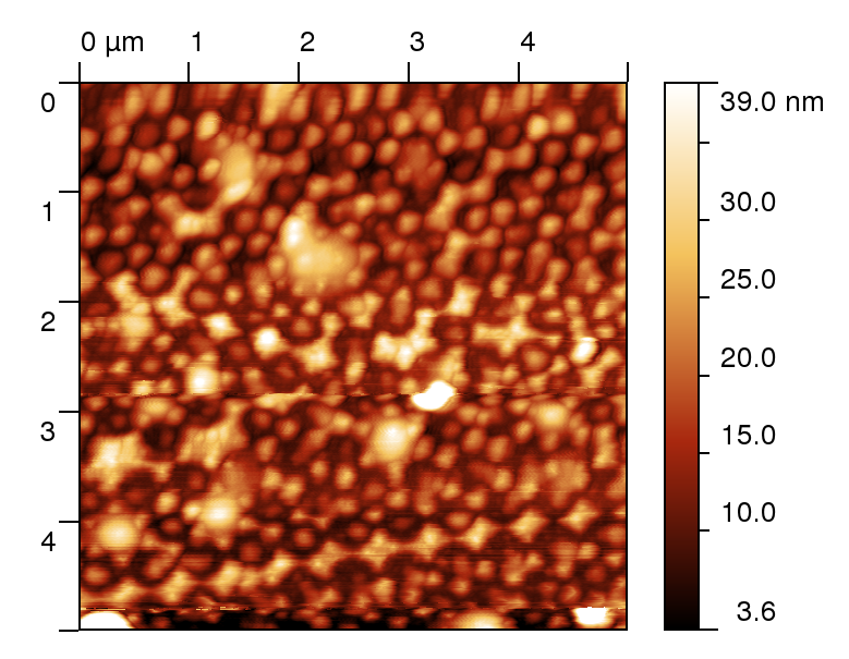
| SNOM image of aluminum islands on glass. |
A solution could be based on a use of apertureless microscopy where the optical probe is replaced by a diffraction on a metal AFM
probe. But also here the data interpretation is not easy and moreover the signal to noise ratio can be higher compared to aperture SNOM.
The result is that currently for optical measurements with high resolution (breaking the diffraction limit) only qualitative analysis is possible. Our aim is to find with the help of FDTD calculations such conditions with the help of which we would get at least some quantitative data with these techniques.
|

