CMI
About nanometrology
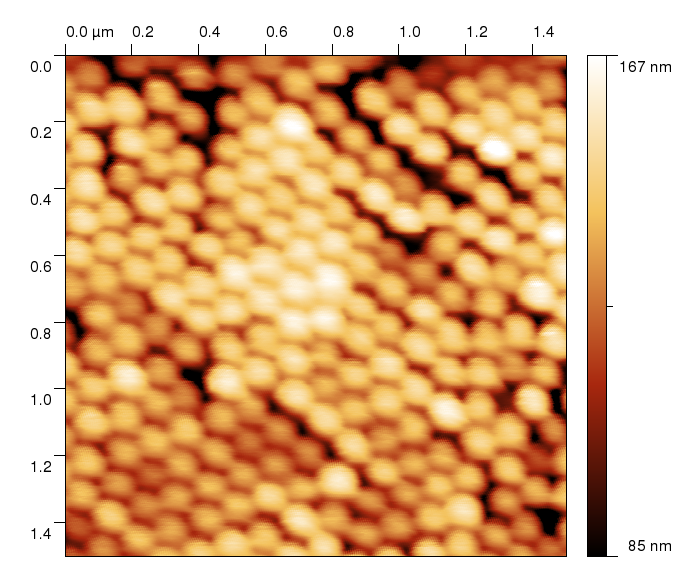
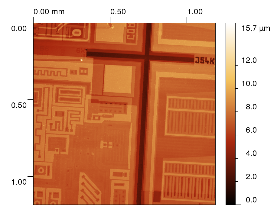
Morphology measurement
Volume structure
Mechanical properties
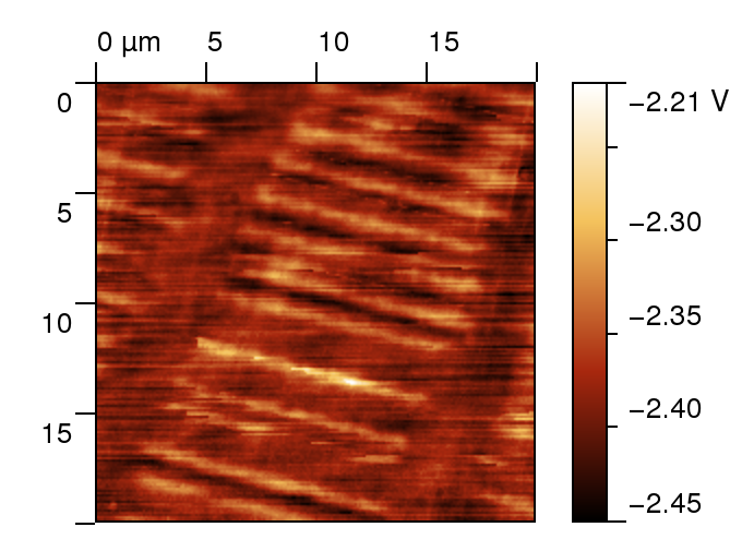
Electric/magnetic properties
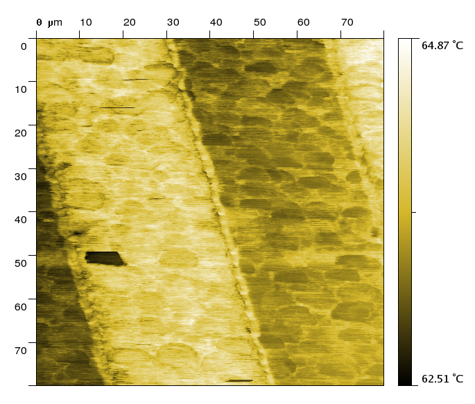
Thermal properties
Local chemical composition
Optical properties
Research
Development of instrumentation
Quantitative SPM
Software development
Traceability provision
Techniques
Atomic Force Microscopy
Electric current mapping
Electric and magnetic fields
Thermal microscopy
Scanning optical microscopy
Services
Surface morphology
Roughness and waviness
Other physical quantities
Hardness, mech. properties
Gallery
Download
References
Partners
Contact
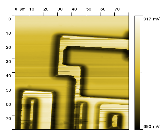
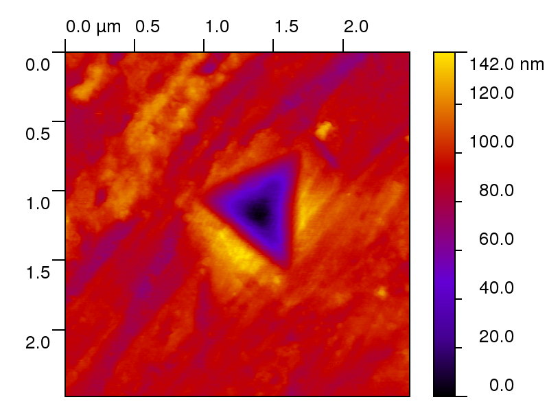
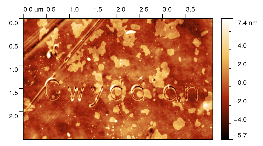
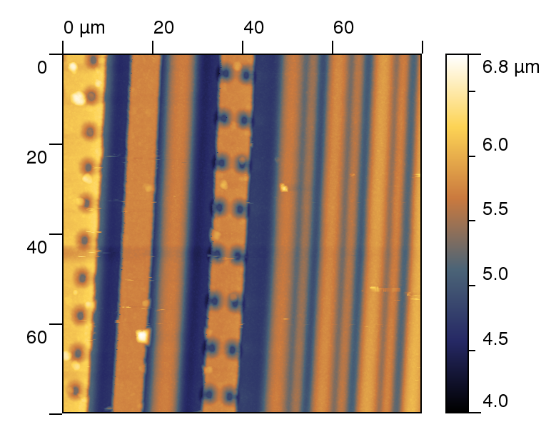
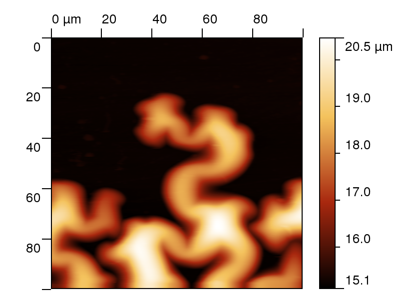
SPM measurements gallery
Nanometrologie.cz
Powered by,
UberGallery
(c) CMI 2012
News
Book of abstracts from SPM workshop 2025 in Lednice is available
here
.
Contact
Department of primary nanometrology and technical length
Czech Metrology Institute
Okružní 31, 638 00 Brno
petr.klapetek(at)cmi.gov.cz


.png)
.png)
.png)
.png)