Quantitative SPM measurements
Surface morphology and mechanical properties measurement
If we focus on objects bigger than ca 10 nanometers quantitative measurement of the surface topography is probably the easiest discipline of the
scanning microscopy technique. Although acquired data are influenced by the tip-sample convolution and can be affected by different systematic errors (calibration)
or random phenomena (noise), detection methods and potential compensations of these phenomena are generally known and can be accomplished basically in every SW
for SPM data analysis (e.g. Gwyddion).
If we want to measure objects which are smaller the situation is more complicated. We cannot expect that the objects are infinitely stiff
and we have to supplement the measurement with a numerical modeling of the tip-sample interaction including the forces acting between the tip and the sample as well as
reversible and irreversible deformations of both bodies. Only this approach can give us an information about the contributions to the uncertainty budget which have origins
in quantum mechanical phenomena occurring between the tip and the sample.
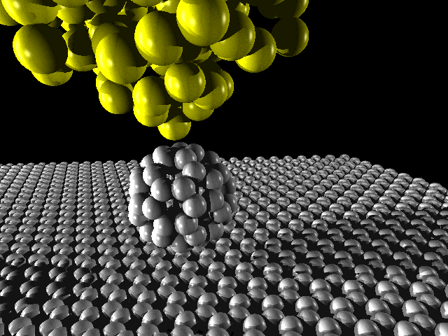
The most natural way of how to address the phenomena between the tip and the sample is to use some of the ab-initio methods, e.g. the
density functional theory (DFT). In case of a limited number of particles we are able to calculate forces as well as mutual positions and final shapes of individual bodies.
In our department, we have a collaboration with the Institute of Physics ASCR in this field and we are using Fireball code which is adapted in
a great manner for computations in the field of scanning microscopy. The result of the computation is an information leading to a uncertainty determination during
scanning of different nanoscale objects and evaluation of forces acting between them [1,2].
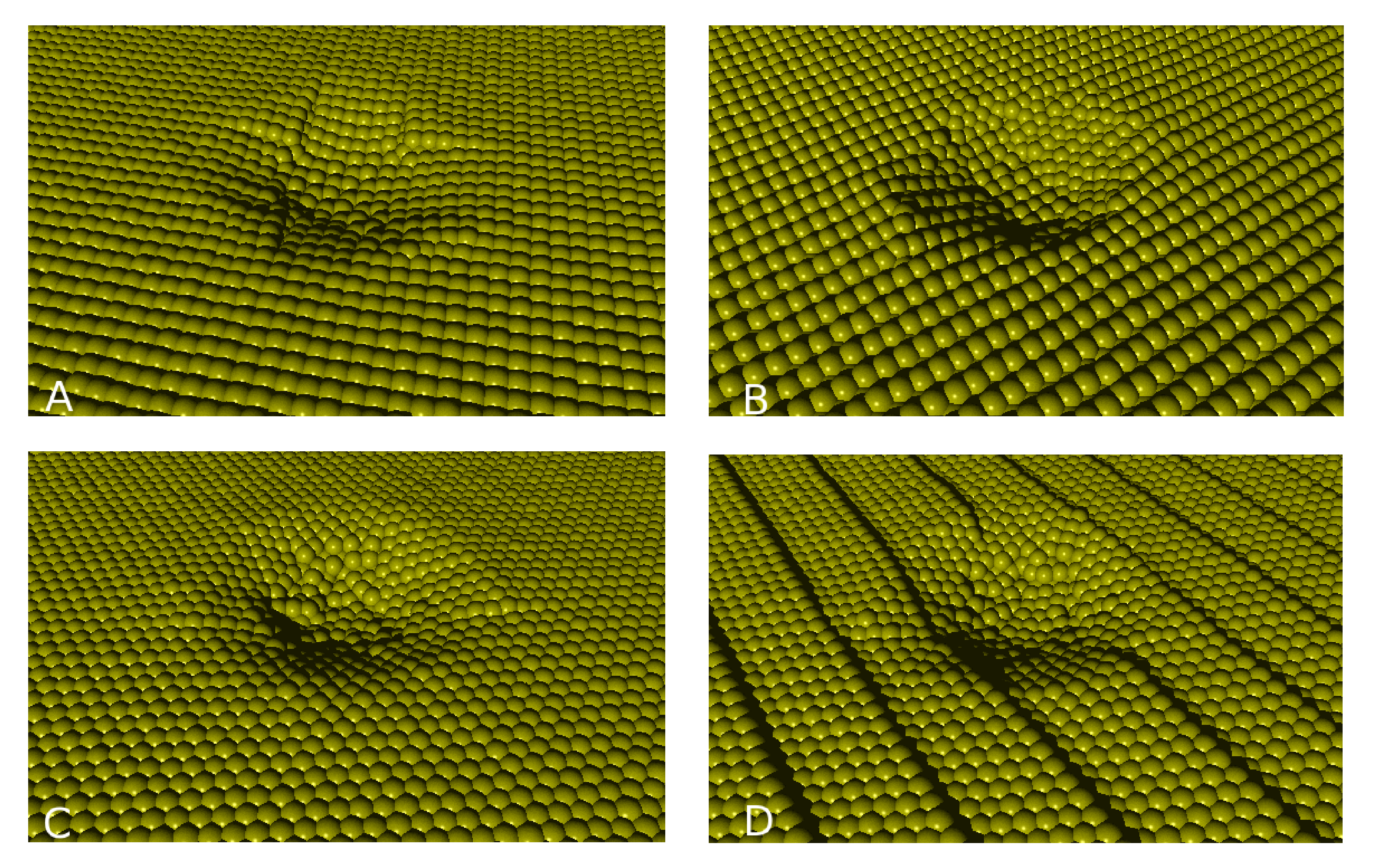
In many cases we have to analyze by far the larger structures than is possible with the DFT. Therefore, we have to decrease our demands on the correctness
of the calculations and use a approximate method, e.g. classical molecular dynamic. Quantum mechanical interactions are reduced on simple analytic potentials by this way
enabling us to perform calculations on hundreds of millions of atoms instead of thousands of atoms. Besides nanometric structures we can simulate also spatially large phenomena,
e.g. in the field of nanoindentation [3]. In the Department of Nanometrology we are using our own molecular dynamics software capable of running not only on the processor
of a personal computer but also on the computer graphics card benefiting in substantially higher speed of calculations.
 |
 |
| Configuration of the interaction between the AFM tip and fulerene (C60) during DFT/MD computations. |
Simulation of indentation into a gold crystal having different surface orientations. |
Thermal, electric and magnetic phenomena
During an analysis of quantitative data acquired by different special SPM methods such as electric or thermal microscopy it is nearly always necessary
to perform a numerical analysis. Often, it is necessary to develop special methods for data acquisition itself which could be compared to numerical experiments.
Typically used numerical methods are the Finite Element Method (FEM) and the Finite Difference Method (FDM) which are used to solve equations suitable for a description of a
particular measurement (Poisson equation is used in case of thermal and electrostatic phenomena, Landau-Lifschitz-Gilbert equation is used in case of magnetic phenomena).
For calculation of these phenomena we use our own software as well as open source SW such as Sfepy, Elmer or OOMMS.
In certain cases the amount of information about the properties of the tip-sample system is so small that is problematic even to setup the model.
In such a case it is possible to use some of the approximate methods, e.g. signal prediction by the neural network [4].
Such an approach is especially appropriate for a study of different artifacts typical for SPM measurements.
 |
 |
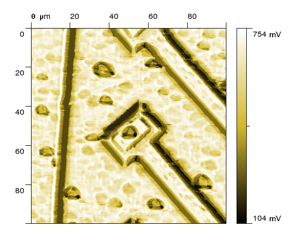 |
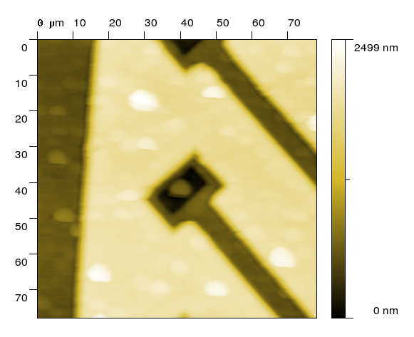
| surface morphology |
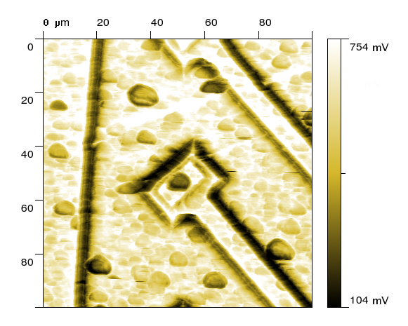
acquired thermal signal (SThM) |
predicted thermal signal (neuron network) |
Optical microscopy
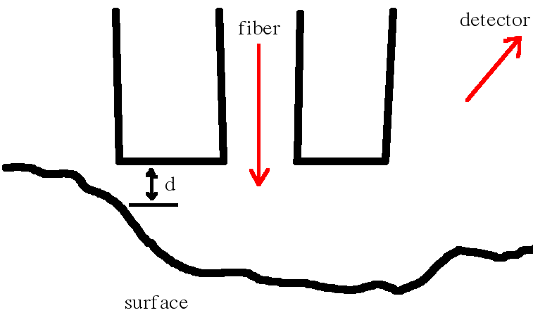
In near-field scanning optical microscopy (NSOM or SNOM) it is almost impossible to perform quantitative measurements without any numerical analysis (and
it is often impossible even with it). For this purpose we use the FDTD (Finite Difference
in Time Domain) method with the help of which we can simulate the distribution of the electromagnetic field in the space between the probe and the surface and, consequently,
in the far field where the detector is typically situated [5]. This method is suitable not only for the uncertainty analysis of the SNOM technique but also for the
understanding data acquired on unknown structures [6].
For the FDTD calculation we are using our own software also capable of running on a computer graphics card. This software is gradually modified into
a open source package for optical calculations Gsvit. The application of the FDTD method is much broader than just an evaluation of SNOM
images, in our department we are using it also for an analysis of dispersion [7], solar cell analysis [8] or an analysis of microstructures created by lithography [9].
 |
 |
 |
| Geometry of a FDTD calculation |
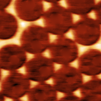
Acquired morphology (aluminum islands) |
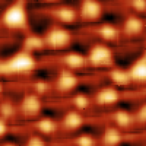
Simulated reflectance SNOM image |
[1]A. Campbellová, P. Klapetek a M. Valtr,
Tip-sample relaxation as a source of uncertainty in nanoscale scanning probe microscopy measurements,
Measurement Science and Technology, 20, 2009, 084014
[2]A. Campbellová, M. Ondráček, P. Pou, R. Pérez, P. Klapetek and P. Jelínek, 'Sub-atomic' resolution of non-contact atomic force microscope images induced
by a heterogeneous tip structure: a density functional theory study, Nanotechnology 22, 2011, 295710
[3]A. Campbellová, P. Klapetek, V. Buršíková, M. Valtr, J. Buršík, Small-load nanoindentation experiments on metals,
Surface and Interface Analysis, 42 2010, 6, pp 766-769
[4]P. Klapetek, I. Ohlídal and J. Buršík: Application of scanning thermal microscopy in analysis of the geometry of patterned structures,
Surface and Interface Analysis 38 (2006) 383-387
[5]P. Klapetek, M. Valtr: Near field optical microscopy simulations using graphics processing units, Surface and Interface Analysis 2010, 42, pp 1109-1113
[6]P. Klapetek, J. Bujdák, J. Buršík: Near-field scanning optical microscopy local luminescence studies of rhodamine dye,
Central European Journal of Physics 8 (2010) 312-317.
[7]P. Klapetek, M. Valtr, A. Poruba, D. Nečas, M. Ohlídal, Rough surface scattering simulations using graphics cards, Applied Surface Science 2010, 256, pp 5640-5643
[8]A. Poruba, P. Klapetek, J. Holovský, A. Purkrt and M. Vaněček, Experimental Limits of Light Capture in Thin Film Silicon Devices,
MRS Proceedings, Vol. 1101, 2008, DOI: http://dx.doi.org/10.1557/PROC-1101-KK02-03
[9]P. Klapetek, T. Wágner and J. Orava, Electromagnetic field distribution modelling in microlenses fabrication process,
Journal of Physics and Chemistry of Solids, Volume 68, Issues 5-6, May-June 2007, Pages 887-890
|

